Physicists encrypt and transmit information with the help of quantum cryptography, a communication protection method wherein quantum objects, such as single photons, are used to transmit and receive information via optical channels. With this method, data storage and transmission can be more secure: if a malefactor attempts to intercept the photon, its quantum state will change and the addressee will know that the system has been compromised.
However, single photons are not easy to acquire: currently, it can be done with the help of suppressed laser radiation or semiconductor quantum dots. In the first case, the radiation is suppressed to the point where, statistically, one laser pulse only emits one photon – this is not the most precise method, so one pulse can contain more or less photons than needed. The second method relies on quantum dots, which are produced using complex, expensive equipment.
Another promising method of creating single-photon emitters is based on the deformation of two-dimensional semiconductors with the probe of an atomic force microscope. The resulting emitters are very bright, produce only one photon at a time, are easy to manufacture, and have the potential to be used at room temperature. However, it is still unclear how two-dimensional emitters can generate single-photon radiation, which makes it challenging to apply these structures in quantum technologies.
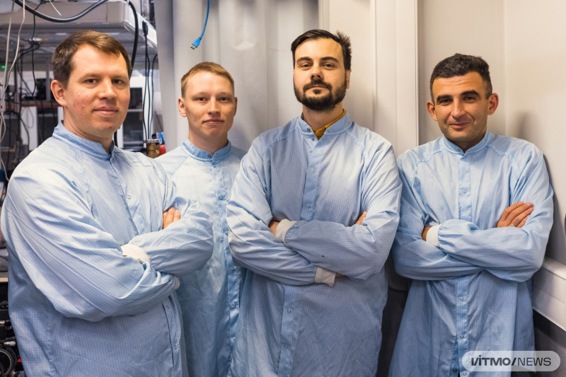
Left to right: Vasili Kravtsov, Artem Abramov, Igor Chestnov, and Ivan Iorsh. Photo by Dmitry Grigoryev / ITMO.NEWS
A solution from ITMO
At ITMO, researchers have analyzed the formation of single-photon emitters in deformed two-dimensional semiconductors and learned to precisely identify their location in the structure. In their experiments, the team has demonstrated for the first time how such emitters (just a few nanometers in size) can be located with the precision of up to tens of nanometers.
Moreover, the researchers have identified the deformations that occur at the spot where an emitter is formed. According to the acquired data, single-photon emitter formation is connected to point-like defects in the semiconductor monolayer. These defects activate when the monolayer’s crystalline lattice is stretched to a specific point.
Single-photon emitters analyzed by the team are very bright, emit only one photon at a time in 98% of cases, and are easy to manufacture.

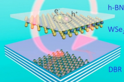
In the experiment, the researchers deformed a WSe2 semiconductor monolayer. This monolayer possesses atomic defects: cells that don’t contain atoms. In the cells where the deformation reaches the necessary scale, quantum light is produced, creating a single-photon emitting system. Credit: Nature Communications
What’s next
The results of this study make it possible to produce single-photon emitters on optical chips with nanometer precision and incorporate them into nanophotonic structures, thus contributing to the development of quantum communication and computation devices.
“We were able to non-invasively locate quantum emitters with the precision of up to 30 nanometers. This technology will make it possible to integrate such emitters into complex chips with nanophotonic structures and control their optical properties. Fundamentally speaking, we have calculated the deformations and proved a theoretical model that suggests that quantum emitters form at the sites of optical transition. The latter appear on atomic defects due to deformations in the crystalline lattice of the semiconductor monolayer,” says Artem Abramov, one of the paper’s authors and an engineer at ITMO’s Faculty of Physics.
In the future, the researchers are planning to integrate a quantum emitter into a nanophotonic resonator that would make the emitter even brighter while also improving the control over the direction of its radiation. Such structures could be used as components in quantum information transfer and encryption devices, as well as other equipment for quantum computing and probing.
This project is supported by the national program Priority 2030.
Reference: Artem Abramov, Igor Chestnov, Ekaterina Alimova, Tatiana Ivanova, Ivan Mukhin, Dmitry Krizhanovskii, Ivan Shelykh, Ivan Iorsh, Vasily Kravtsov. Photoluminescence imaging of single-photon emitters within nanoscale strain profiles in monolayer WSe2 (Nature Communications, 2023)