Your family is an example of a scientific dynasty – your father was born into a family of engineers. Did that influence his decision to do research?
My paternal grandmother was a forestry engineer who developed a system for timber collection and distribution via rope- and railway. Her second husband was also an educated man; he spoke Greek and German and also taught me French. He was a train engineer, but during the war he repaired combat aircraft after battles. After the war, he developed special paper for Goznak (the state enterprise responsible for manufacturing banknotes, secure documents, etc. – Ed.). I think seeing all this, my dad had a clear idea of what engineering is and that’s why he chose his career.
Why did your father opt for optics?
My father studied at the Faculty of Physics and Engineering at LITMO, where he met his wife, Galina. After graduation, father got a position at the S.I. Vavilov State Optical Institute, a major institution with around 15,000 employees.
As a recent graduate, he couldn’t get a position higher than a regular engineer – to move up the career ladder, he needed a PhD. That’s why he decided to get one at the institute. His supervisor Evgeny Yudin picked optics as the topic, because my father said he had a passion for photography. Back then, everything about photography was already known, but holography was in its cradle. There was Gabor’s method for producing holograms, but a lot remained to be studied about this topic. So, that became the field my father ventured into.
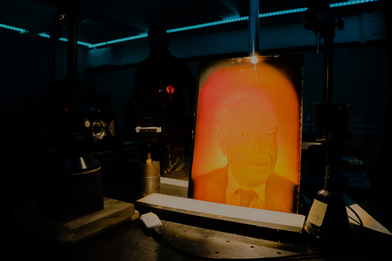
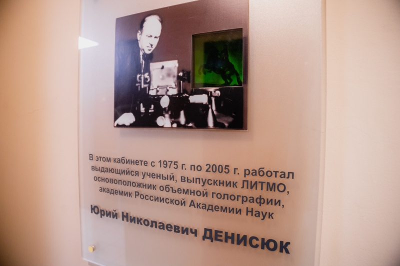
Yuri Denisyuk at work in his lab. Photo courtesy of Historical Museum of ITMO University
Today Yuri Denisyuk is known all over the world as the creator of a method for image recording in 3D environments. Thanks to this method, it is now possible to record full-color ultrarealistic holograms. What did he himself tell you about his work? Did he know right away that he’d made a great discovery?
It wasn’t an easy research project. My father’s supervisor passed away without having the chance to see his student defend his thesis. It was a great personal and professional loss, because a supervisor is the one who guides a young researcher and helps with applying for patents, writing articles, and finding references. Whereas today another supervisor would’ve been appointed for my father, back then the rules weren’t so strict and my father was left to his own devices.
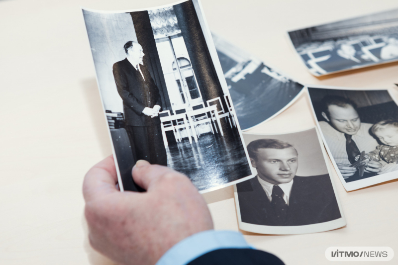
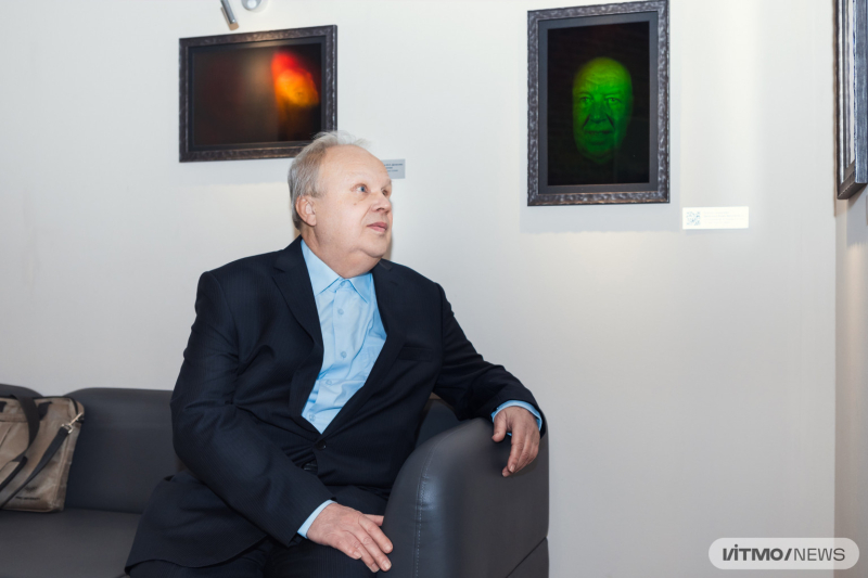
Photos from the Denisyuk family archive. Photo by Dmitry Grigoryev / ITMO.NEWS
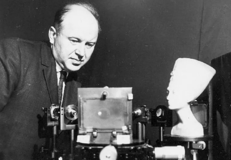
At the institute, my father worked on secret projects, which he couldn’t publish or defend as his thesis. That’s why he decided to keep working with holograms: he laid out all the theory that he needed to test experimentally, but his idea wasn’t supported by the administration. Nevertheless, father was assigned a space where he could conduct his research outside his working hours. He didn’t have access to lasers, so his first images were recorded with a mercury lamp.
Once he documented the results of his studies, he wanted to publish them, but his paper wasn’t accepted because it didn’t reference any prior works on holography. This was a precarious situation because it was impossible to defend a PhD title without publications – and without the degree, my father could lose his stipend and his job. Eventually, upon advice from physicist Vladimir Linnik, my father corrected his paper, adding only one line, and was able to publish it in 1962.
His defense also proved to be a challenge. My father was really nervous and at one time he even couldn’t speak, so his work was partly presented by his wife. By a margin of one vote from the committee, he was awarded a PhD title. Right after, he was appointed the head of a new laboratory at the institute and issued a state award.
Excerpt from Yuri Denisyuk’s work My Path in Holography:
“I had the daring idea: what if we could make such a photo using modern optical tools? Or rather, could we make a photo that would create a full illusion of reality of the scene it depicts? The first steps are simple. It was clear that in order to fully trick human visual perception into believing it sees an actual object, we would need to fully recreate the wavefield of light scattered by this object. It was also clear that this task would be solved if we could find a method to record and reproduce the phase distribution of this wavefield. At the time, as I wasn’t aware of Gabor’s method and the term holography, so I called this process “wave photography.”
For a while, holography remained forgotten in Russia, until my father’s paper was translated into English. In 1968, he was invited to deliver a report at a holography conference in Paris– a rare, unimaginable offer. After that, it was evident that holography had to be developed in the country and in 1970 a laboratory of holography was opened at the S.I. Vavilov State Optical Institute and headed by my father. Later, he got the title of DSc and became a corresponding member of the USSR Academy of Sciences.
After leaving the S.I. Vavilov State Optical Institute in the mid-1970s, my father became a researcher at the Ioffe Institute. And in 1996, he was invited as a lecturer on holography to ITMO by Rector Vladimir Vasilyev.
A classroom at ITMO. Photo by ITMO University
What’s the greatest piece of advice you’ve received from your father?
Just like my father, I was a child of engineers. I would often visit them at work and gawk at various optical devices that greatly interested me. Dad supported all of my research endeavors. For instance, once, we held our own experiment with different conditions at home based on a piece about vortex generators I read in a teen tech magazine.
My dad taught me to study every unknown fact in different situations to see what it depends on. That had a great impact on my choice of career.
Here’s how my father described the meaning of research: engineers need to follow the set guidelines to make something; however, sometimes, we discover something new – that’s what science is about. Sometimes, there are articles on a particular topic and we can recreate the experiments they describe. At other times, it’s not clear how to do something. We need to see who did something similar and try different approaches. And sometimes, you discover an artifact – a phenomenon that doesn’t fit into the existing paradigm. Some wouldn’t see it as a discovery, while others would see the potential in it and start developing this topic. This way, one by one researchers will pour themselves into a field, polishing the existing concept to completion.
I thought to follow in my family’s footsteps and become an engineer, but my father advised me to study microelectronics. I graduated from LETI University, then worked at the S.I. Vavilov State Optical Institute, and later – at ITMO.
Igor Denisyuk. Photo by Dmitry Grigoryev / ITMO.NEWS
You’ve spent over 20 years at ITMO, having founded the research school of hybrid optical nanostructured materials. What was your research about and what results were you able to produce?
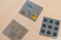
Apart from giving lectures in photonics, biophysics, nanotechnologies, and nonlinear optics, I headed over 35 projects. For instance, for Goznak I developed polymers with high concentrations of nanocrystals, which I used to make more resilient holograms that can remain intact even after being boiled or ironed. Thanks to this property, such holograms can be used as an anti-fraud protection system on documents.
I’ve also developed an electro-optical modulator based on DAST organic crystals. This device can process signals from radars: they are sent to electro-optical modulators, which modulate a light signal by regulating the amplitude, phase, and polarization of radiation. The filtered light signal is then processed by a regular digital device. Such modulators are used in optical systems to process, encrypt, and decrypt signals.
Which of the projects you started are currently developed at ITMO?
I have several successors, one of whom is Maria Fokina. In 2003, she became my student and later went on to defend her PhD thesis. She is now an associate professor and the head of my former laboratory of nonlinear crystals at ITMO. Recently, we developed an assembly line with computer vision for automatic sorting of amber based on the type of stone. The second recent project concerns the development of polymers with silver and zinc oxide in collaboration with Kashkin Research Institute of Medical Mycology. We studied the way our materials suppress various microorganisms and fungi to see whether they can be used in wound healing.
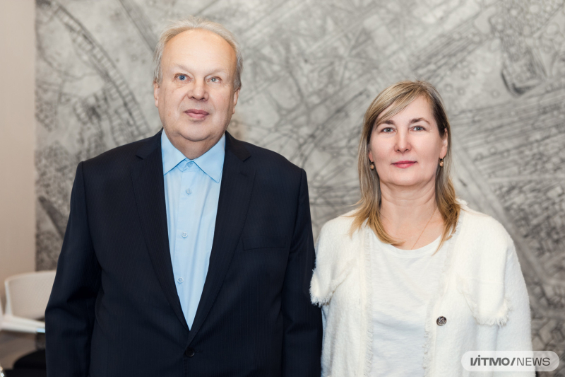
Igor Denisyuk and Maya Uspenskaya. Photo by Dmitry Grigoryev / ITMO.NEWS
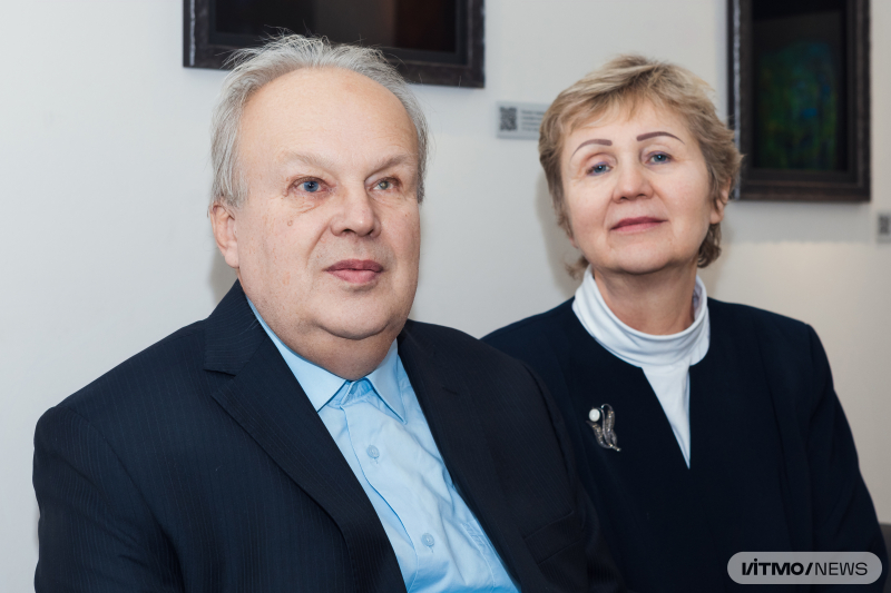
Igor Denisyuk with his wife Tatyana. Photo by Dmitry Grigoryev / ITMO.NEWS
Maya Uspenskaya, the head of the Center for Chemical Engineering, is another colleague and research partner. We met at a thesis defense and started collaborating. She has also developed a medical solution – a hydrogel wound coating with nanoparticles that suppress microbes and fungi, facilitating tissue regeneration. Another field she is working on is bone transplants: according to Dr. Uspenskaya’s vision, in the future, you won’t need to look for a bone donor – instead, you’d be able to introduce a nanocomposite that will gradually regrow the bone. After the job is done, the nanocomposite will degrade on its own.
My son Andrey is also a researcher, but he has a more industry-oriented approach. Currently, he is developing nanolithography machines, providing technical support, and training employees.
What do you think is needed to create and support succession in science?
In order to do this, you would first need a specialist who has experience, publications, achievements, and the desire to teach others. This specialist will share their experience, conducting research with their students. Then, their trained graduate will not necessarily stay in the same university, moving on to other places to gain more experience, and then find a new place of work. And this is succession. I have supervised 11 PhD candidates who defended their theses; the majority of them became heads of laboratories at major companies.
To all young researchers, I wish this: may they see new horizons and find their paths in science and technology to develop new devices and make new discoveries. Best of luck!