Transistors are miniscule semiconductor devices that control the flow of electrons as it delivers data – with every year, these devices become smaller and more efficient. After all, they are critical to the efficiency and performance of any digital tech, including smartphones and computers. However, the fundamental limits to their productivity have nearly been reached. Now, their performance can be improved by basing them on photons (light particles) instead of electrons. As a means of information transfer, photons are ideal: light can travel over tens and even hundreds of kilometers without fading or distortion. And this is exactly why optical computers are not just a scientific endeavor, but an actual necessity.
“To develop a functional optical computer, we need to replace every part of a conventional PC with its optical counterpart. In our project, we were able to create, in a sense, a building block for a future optical chip: a nanostructure that can serve as a condenser or even a semiconductor. The structure can also be used to control the flow of photons: for instance, change the intensity or direction of radiation. Moreover, we were able to generate a consistent electric field inside the nanostructure using only light, without any electrodes or additional electrical systems,” says Yali Sun, the article’s first author, a junior researcher at ITMO’s Faculty of Physics.
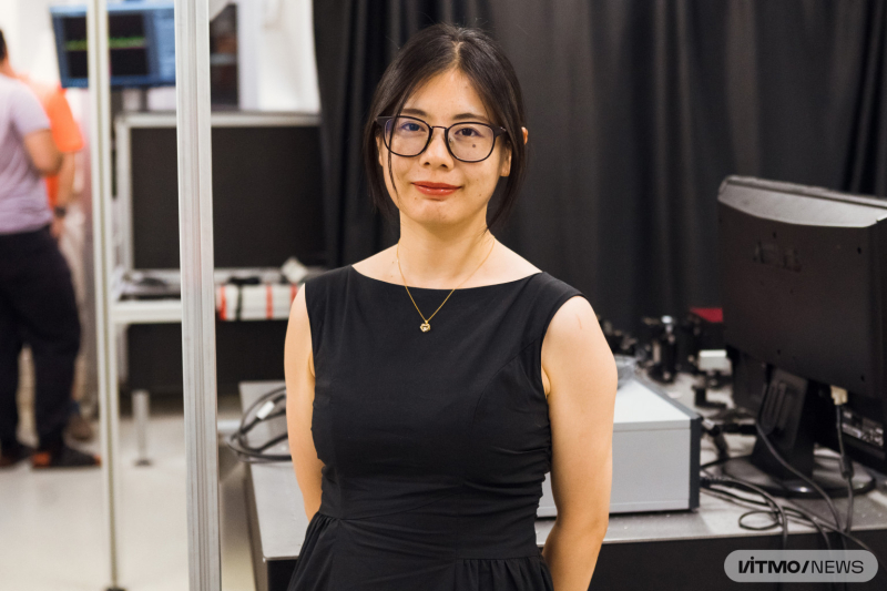
Yali Sun. Photo by Dmitry Grigoryev / ITMO.NEWS
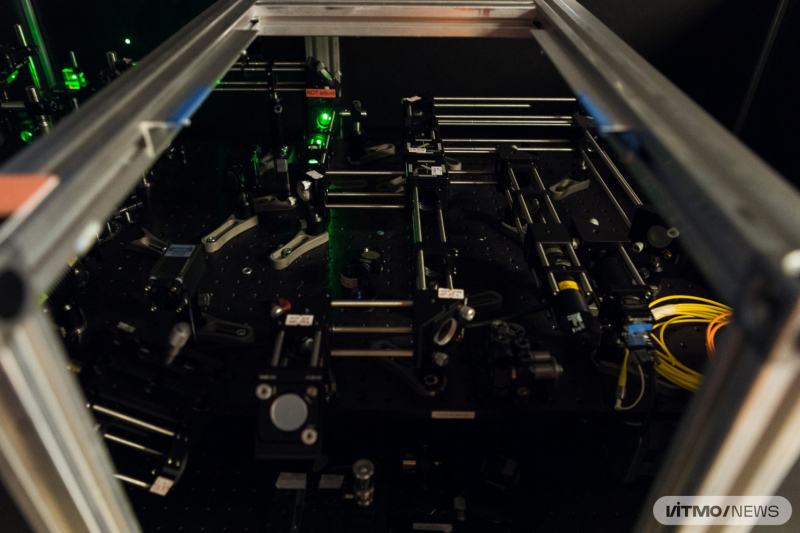
The optical system for the study of optical response in nanostructures. Photo by Dmitry Grigoryev / ITMO.NEWS
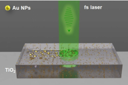
Miniaturization was another task the researchers were trying to tackle: the smaller the structure, the more densely packed it is with potential transistors – thus the more powerful the final device. In this project, the team was able to use laser radiation to generate a static electric field inside the structure without using any electrodes. This was possible because of the structure’s optical resonance properties and the use of two materials within a single nanosystem. Previously, this effect was only demonstrated in bulky systems, such as 3D silicon.
“Our nanostructure somewhat resembles a chess pawn: it’s a truncated cone topped with a sphere. We have experimented with nanostructures of various geometry to demonstrate that this exact shape is the most suitable for generating an electric field. The nanostructure contains materials widely used in microelectronics – silicon and gold. Here’s how it works: we expose it to a laser and thus generate an electric field inside the semiconductor; the field then changes the nanosystem’s optical response. So, effectively, the output radiation of this nanostructure can be controlled with light. This is an important feature for photon-photon interaction. The results of our study will contribute to the development of optical computers where all processes are accomplished with photons,” explains Artem Larin, a co-author of the paper and an engineer at ITMO’s Faculty of Physics.
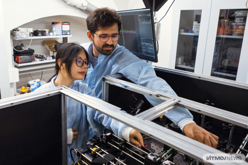
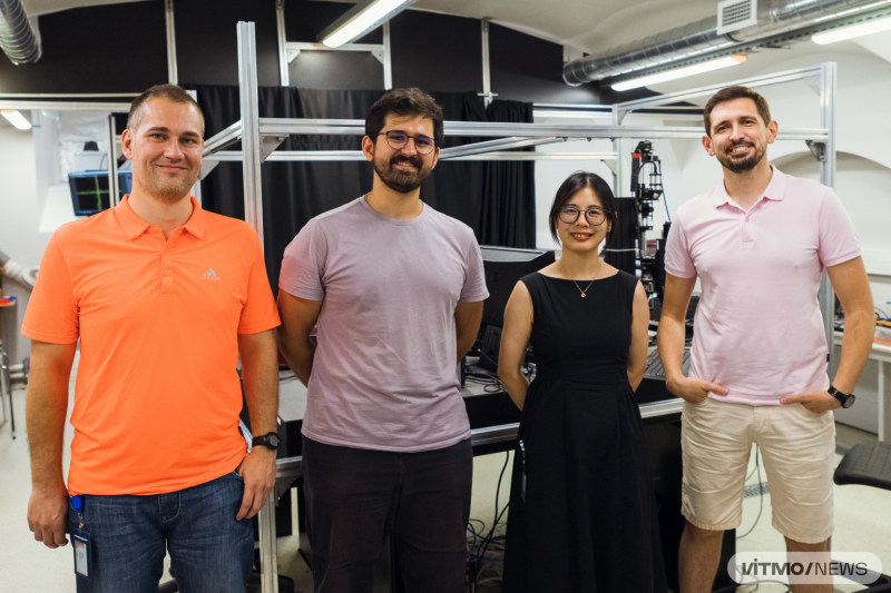
Yali Sun and Artem Larin. The experimental study of hybrid nanoantennae. Photo by Dmitry Grigoryev / ITMO.NEWS
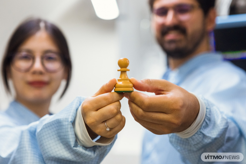
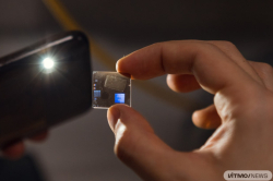
The device developed by the researchers is shaped like a chess pawn. Photo by Dmitry Grigoryev / ITMO.NEWS
According to Dmitry Zuev, the supervisor of the project and a senior researcher at ITMO’s Faculty of Physics, the toughest part of the project was providing theoretical descriptions for the results obtained in experiments. This is because the theory describes an ideal case, with no account for a plethora of factors. Next, the physicists are planning to experiment with other geometries in order to improve the methods of creating such nanosystems.
ITMO's Press Service