How did you start working with metamaterials?
I began my work in this field in America back in 1997. At that time, we developed carbon nanotube synthesis and its applications. Now I work at the Texas University in Dallas. Before moving to America, I lived in Japan, where my work focused on producing superconductors and magnetic materials from fullerene. I was the first to create photovoltaic batteries from fullerene.
When I moved to America, I started working for the HoneyWell company which was later bought by General Electric. Thus, we were to merge with their research center. Many of us didn't like it, so when some wealthy benefactors from Texas offered us to organize our own institution, we agreed. They gave us the necessary money and opportunities, and we built a nanotechnologies institution from scratch.
What are the materials you commonly work with?
We work with advanced materials, including perovskites, and work at the intersection of Materials science, Physics, Chemistry, and Biology. Perovskites are complex structures, named after a Russian researcher count Lev Perovski. In 1839, perovskites were discovered in Ural mountains. Those were not identical to ones we synthesize now but are the progenitors of the current structures.

Perovskite. Credit: http://geo.web.ru
The natural perovskites' formula is CaTiO3, and the ones we produce are called hybrid organic-inorganic halide perovskites. They are great for creating different materials and devices, but very delicate - even a drop of water can dissolve them. This is why we conduct our research in special boxes.
What research is the new laboratory currently working on?
In the first place, we have to learn to "grow" the materials we study, as its hard to conduct experiments when someone else creates your samples. Only after you've learned to create materials, you can effectively study them and create new devices.
Before I brought the technology for creating perovskites to Russia, no one really researched them here. At first, I shared the knowledge with my colleagues from MISIS, where I've been working for two years on a grant project. Several years later, I gave a lecture at ITMO's Metamaterials laboratory and got interested in it. Sergei Makarov, the current co-head of our project, came to my laboratory in the USA, and we've been actively collaborating ever since.
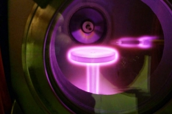
 Laboratory of Hybrid Nanophotonics and Optoelectronics
I became really enthusiastic about combining the perovskites from my laboratory with what scientists work on at ITMO University - resonant nanoparticles with high refraction index and other nanostructures created at the Metamaterials laboratory. To make the collaboration even more effective, we've launched the new Perolab laboratory (the Laboratory of Hybrid Nanophotonics and Optoelectronics -- Ed.), which is fixed with the most hi-end equipment - some of the units are even better than those at my laboratory in the USA. Here, we have the ideal conditions for working with perovskites.
What are your responsibilities as the head of the new grant and laboratory?
As per the contract, I have to spend four months at the laboratory; I think I'll be coming here in the end of May and staying the summer in St. Petersburg. Naturally, we'll constantly be in contact with our staff and students - nowadays, that is not a problem. Students, Ph.D. students, postdocs or other visitors will often come to see me at my lab; we can even keep in touch using Skype. Personally, I sometimes use it to read lectures from home.
 Anvar Zakhidov at ITMO University
What has been done in the laboratory over the past year?
We've developed two devices based on my concepts. One is a perovskite-based solar battery that can work both as a power source and a display. As of now, there's a similar product on the market - a display (like the one you have on your smartphone) with an OLED screen which uses organic LEDs, and a common solar cell. It has a switch that allows it to work either as a battery or as both battery and display. Let's say you drive your car, and the display is fixed to your windscreen. Its one side absorbs solar energy, and the other shows you different data: temperature, time, speed, etc.
The other invention is luminant LEDs based on a simple polymer-perovskite structure. Common LEDs gradually go out and change their color. These are based on iodine and bromide. We've added chloride; as a result, we got a pleasant blue light source.
 Laboratory of Hybrid Nanophotonics and Optoelectronics
What do you do at the Texas University in Dallas?
There, I have a large group of scientists who also focus on perovskites. I believe that the creation of nano-imprints is amongst our major achievements, as they possess unique properties. Usually, one would use photolithography to apply patterns on a surface, yet you can't do that with perovskites, as they are dissolved by water.
If we are to create a picture on a perovskite film, we are to use different methods. We use stamps that we apply to the sample, then heat it or apply pressure, thus imprinting the picture. Such pictures can be the size of tens or hundreds of nanometers, less than a micron.
I want to bring this technology to St. Petersburg, as well. At the Metamaterials laboratory, they create nanoparticles, and we can provide them with perovskite nanofilms with patterns so that these particles can be applied to them. I recently published an article on such structures.
METANANO-2017's website. Credit: metanano.ifmo.ru
What did you like about the METANANO conference?
The conference was most rewarding. Since I went from Moscow to Japan and then to America, I haven't been in Russia for a long time. Since then, photonics in Russia made a huge step forward, and I fell behind. At the METANANO conference, I got to know the new generation of young scientists. They show great results, and many distinguished scientists from all over the world that I am familiar with come to see them. Here, I met Boris Lukinchuk from Singapore, Andrei Rogach from Hong Kong, Alexei Kavokin from Germany and many of my other colleagues.
I got interested in the report by professor Franko Nori who spoke about light's spin properties and optical diodes. The presentation took a whole hour, but I listened very attentively. Everything that was discussed at METANANO is the last word in fundamental science. And I want to note that Russia has always been great in everything that has to do with fundamental research.
I was dazed by Vladivostok and the Far Eastern Federal University's campus. Back when I left the Soviet Union and came to Japan, it seemed very modern and beautiful. Now, when I look at the great architecture of Far Eastern Federal University's buildings, I feel that Japan pales in comparison.