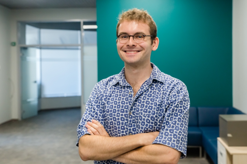
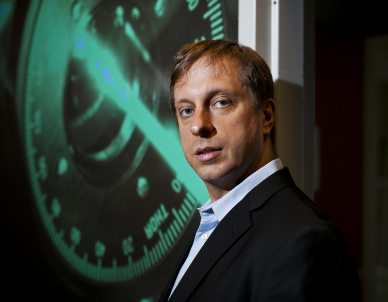
You are currently working with the research team of Marin Soljačić (a professor in physics at MIT; in 2007, The New York Times included him into the list of the 70 authors of exceptional and ingenious ideas). Can you tell us in more detail about your research, please?
I am currently a third-year PhD student at MIT, and I am working in Marin Soljačić’s research team. During my PhD and earlier research experiences, I have come to work on various fields of physics: nanophotonics, light-matter interaction, free-electron physics, nanophotonic computing, and machine learning.
When I was a research intern at the John A. Paulson Harvard School of Engineering and Applied Sciences (SEAS), I worked under the supervision of Prof. Federico Capasso on dielectric metasurfaces. When joining MIT for my PhD studies, I slightly shifted my research focus.
Broadly speaking, I now work on light-matter interaction mediated by free-electrons, and nanophotonic computing applied to machine learning and NP-Hard optimization. I conduct both theoretical and experimental research. In the former, I perform experiments where we excite nanophotonic structures (such as photonic crystals, nanogratings, etc) with free electrons, in order to generate radiation. If we want to improve the interaction between free electrons, light, and matter, we need structures with featured properties. Dielectric nanostructures are a very interesting area of research to design such interesting properties (one simple explanation is that lossless dielectric structures offer the possibility of confining light very efficiently).
What are the possible applications of this research?
One application of such photonic structures is to enhance light-matter interaction, for instance with free electrons. We can thus apply these concepts to the development of novel integrated, tunable light sources. So, for instance, one thing we have developed at MIT recently is an integrated near-infrared source made of pure silicon substrates or dielectric structures excited by free electrons. Instead of using the structures we have used at MIT for a proof of concept experiment, a possible continuation of this work is to use high-quality factor structures that we are currently developing in the group of Andrey Bogdanov. These ideas were suggested in a paper our group published in Nature Physics last year.
You say that you’ve done research in fields other than photonics. How exactly did you begin your career in science?
I was originally born in Besançon, a medium-size French town not far from the French-Swiss border. There, I graduated from highschool, and then went to Paris to complete preparatory classes for the French Grandes Ecoles. In the end, I joined École Polytechnique in Palaiseau, and got my Bachelor’s and Master’s degrees there. This part of my education was more fundamental in its nature and mostly focused on physics and engineering sciences.
Towards the end of my Master’s program, I decided to work on my thesis at Harvard SEAS under the guidance of Federico Capasso on dielectric metasurfaces. I then joined MIT’s Department of Electrical Engineering and Computer Science in September 2016, where I have completed a Master of Science in 2018, and where I am currently pursuing my PhD.
What prompted you to focus on nanophotonics?
I have really enjoyed working in this field, as it combines fundamental concepts to various applications. The fundamental principles of nanophotonics are reasonably simple, and building upon them, one can create complex structures with interesting properties (which reminds me of the game of LEGO, for instance).
Metasurfaces offer new opportunities in controlling and manipulating light, and in recent years, scientists have been actively discussing the prospects of using metamaterials in various fields. Still, what are the issues that scientists still have to solve in this regard?
I believe that in the future, metasurfaces may drastically change traditional optics. What’s more, I think that research in this field will make it possible to make conventional devices much more compact.
There are also many potential applications in augmented and virtual reality with some hurdles along the way, such as the problem of chromatic aberrations.
Most dielectric metasurfaces are optimized to work for a single wavelength and angle of operation. For instance, they will act as a focusing lens. Designing single-layer dielectric metasurfaces that realize arbitrary functions over a large bandwidth (such as the entire visible spectrum) is quite challenging and is an active field of research.
That’s something I have worked on during my time in Harvard SEAS, and it’s also something that I’m currently revisiting with Prof. Marin Soljačić. There are different techniques to achieve these broadband designs, but they are all quite challenging even from the standpoint of simulation and optimization.
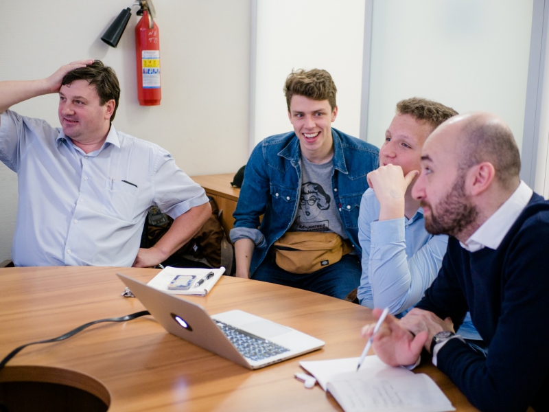
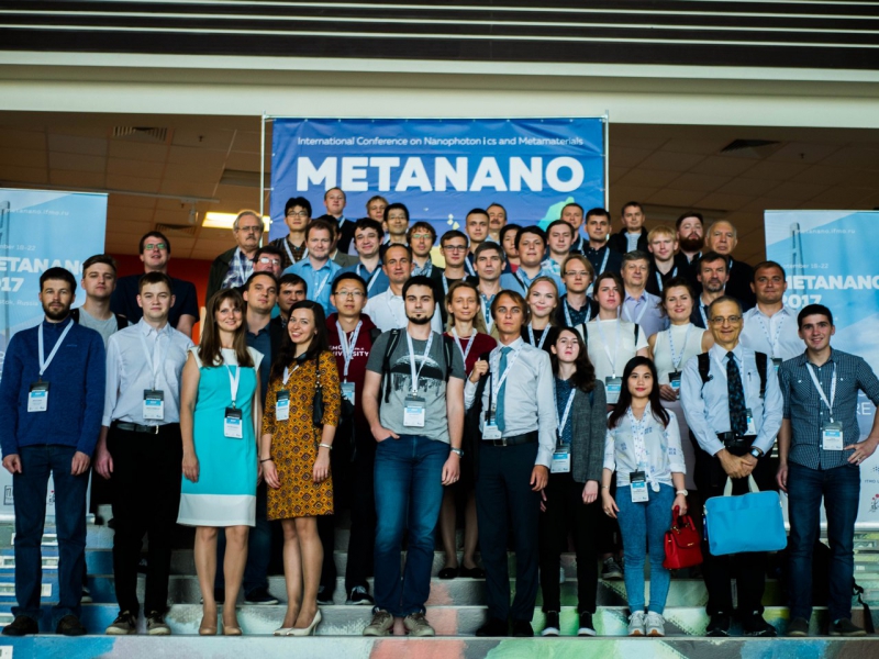
At ITMO University, you are working with Andrey Bogdanov and his colleagues. Why did you choose to come to Russia and work with this research team?
My choice was motivated by several reasons. First of all, I started learning Russian back in my school days in France and continued at MIT, with Dr. Maria Khotimsky. So, I wanted to learn how to use Russian in a professional environment during this internship. I am also very interested in Russian culture: literature, poetry, music, and history. For instance, I have recently gotten interested in translating Russian poetry in French and English, under the guidance of Dr. Maria Khotimsky. Russia is a fabulous country, so I am very glad to have the opportunity to spend my summer here.
Secondly, the team I am now part of is equally famous among those working in the field of nanophotonics. And I think that this internship is a great opportunity to combine my love for the Russian language and culture with my scientific interests. I also had the privilege to benefit from funding offered by MISTI-Russia, an organization that sends students to different Russian universities and companies every year. They made my stay in Russia possible and I would like to thank them for this great opportunity.
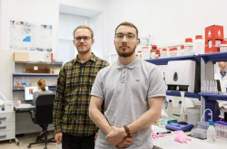
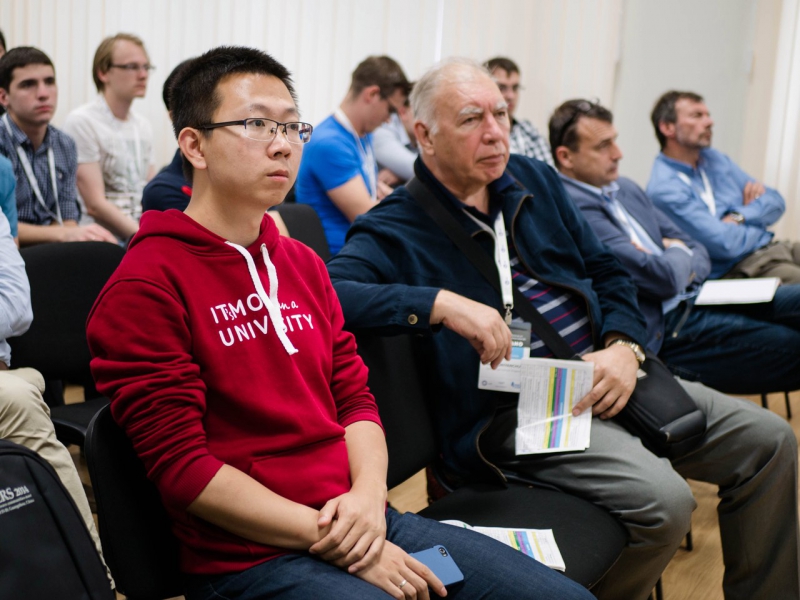
Here at ITMO, I work with Andrey Bogdanov’s team and do both theoretical research and simulations, with the hope of confronting our predictions to experiments by the end of the summer. This work is aimed at designing novel nanophotonic structures with very high-quality factors that are potentially robust to disorder. I hope that this internship is just the beginning of a long and effective collaboration between our team at MIT and scientists from the Research Center of Nanophotonics and Metamaterials.
Back at school, why did you decide to learn Russian?
This is a question Russians often ask, and I tend to answer: but why not? In truth, the original reason was that my grandmother was from Ukraine. She passed when I was just a kid, so I never knew her well. Still, when I grew up, I thought: “Why not find out some more about my origins, and try learning Russian?”.
I then realized that it was a very challenging and interesting language to learn. In some regards, it may be even harder to master than nanophotonics! So, I persisted, and I hope that there will come a day when am able to use it fluently.
Nevertheless, you already use Russian to communicate with your colleagues at ITMO. What was the hardest thing about learning it?
Word stress, I guess. And also the fact that Russians speak really fast, and are not used to taking their time to slow down when speaking to a non-native speaker. You see, in the USA, there are many immigrants, people who are representatives of various nationalities, especially in Boston, which hosts two major universities. There, people are used to speaking slowly and understanding various accents. On the other hand, here in Russia, I get great language practice. By the way, it is the fourth time that I visit Russia, but this is the first time that I stay for so long.
What surprised you the most when you first came to Russia?
Even before my first trip, I read a lot about Russia, so nothing was too surprising for me. I spent the past three years in the USA and got very used to living there. So I can say that I can now compare Russia and the US. In Russia, people tend to smile a little less, but when you get to know them better, you understand that they are very hospitable. In the USA, people are much more friendly at first sight, but getting to know them intimately is sometimes more challenging.
And what’s the difference between working in research teams in Russia and in the USA?
I can only compare it based on my own experience. The team that I work with in the US is quite small, we only have about ten PhD students. Here at MetaLab, the research teams are huge. Nevertheless, since both groups are successful, so I am currently learning more about MetaLab’s operation and management style in such a large structure.
I noticed that the young scientists manage their teams very closely, and pay a great deal of attention to their students.
What are your future plans?
In the future, I would like to work in academia, and in order to achieve this goal, it is very important to understand how to establish collaborations between universities and countries. And I think that my current internship at ITMO offers a great opportunity to learn more about this.