“Big Challenges” summer camp
The “Big Challenges” scientific summer bootcamp for talented high school students was organized by the Sirius education center and took place in Sochi, Russia’s southern resort turned research powerhouse. Winners and high-achievers of the national contest of physics, maths, technologies, and natural sciences research projects were invited to attend. Tutored by leading ITMO scientists, students developed several projects in the fields of big data, nanotechnologies, new materials, cognitive research, World Ocean exploration, satellites, and piloted aeronautical vehicles.
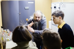
“What was special about the “Big Challenges” summer camp was that it focused on student-led project activities. Participants were given specific tasks which they had to tackle completely on their own. Finding a solution wasn’t easy as it required not only mastering considerable amounts of knowledge and practical skills, but first of all learning how and where to source them. Some of the attendees found it very difficult because they were used to teachers telling them what to do and how to do it. But here you could never be sure about which technology to use for which project, you had to go through a genuine, full-blown scientific enquiry to decide. It made the kids realize that real-life researchers don’t get knowledge delivered to them on a silver platter, they have to work extremely hard,” commented Vladimir Pshenichnov, “Big Challenges” nanotechnologies mentor and associate professor at ITMO University’s Department of Physics.
Camp organizers also attached special importance to teamwork skills development. The students often had to share responsibilities and delegate tasks, which was a first for many participants accustomed to dealing with tasks on their own. Getting to grips with this aspect of teamwork was especially beneficial to students as it taught them to identify their strength and weaknesses in order to effectively share the tasks they were assigned.

“Students presented their projects during numerous joint meetings and the final project fair which featured both project models and promotional materials like posters, prospects, and video ads that were created by the teams. My team’s project was very multifaceted as it touched on a wide range of scientific, technological, economic, social, marketing, and even videography aspects, which in my opinion made it stand out from the rest of the projects. It should be noted that the students I worked with already had a wealth of project work and research experience, so the quality of the projects which they came up with during their time at Sirius resembled that of university students’ theses,” shared Mikhail Zhukov, “Big Challenges” nanotechnologies mentor and engineer at ITMO University’s Department of Nano-Photonics and Metamaterials.
Creating ordered nanostructures arrays
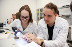
To work on this project, the students joined forces with Mikhail Zhukov and his assistant Polina Shaban, second year student at the Faculty of Physics and Engineering. Today, ordered nanostructures arrays-based templates are becoming more and more popular in modern production cycles as they facilitate the creation of high-brightness light-emitting diode panels, high performance solar batteries, new generation screens, metamaterials, high information density data storage devices, liquid nanofilters used in medical tests, and many other cutting-edge devices. Students based their project on optical photolithography methods with the use of micro and nanospheres. This meant that in order to create an ordered template, the latter was imprinted with a photoresist, a photosensitive material covered with a layer of microspheres.
“Exposed to a plane-mode electromagnetic wave, each sphere turns into a microlens, focusing the incoming radiation on a dot of submicrometer dimensions. This enables us to use the photoresist surface for lithographic processing of submicrometer or nanoscale structure arrays. A simple UV diode is used as a radiation unit. Developing the photoresist deletes the spheres, which in its turn forms an array of micro or nanocavities,” explains Mikhail Zhukov.

To proceed with this project, the students prepared a special room which they had to protect from external light exposure as this could have lead to changes in the photoresist structure and in that disrupted the lithographic process.
Although the students developing this project were only faced with the task of designing a low-cost technology for creating ordered nanostructures arrays, they decided to take it a step further and came up with a prototype of a nanofilter that could be used for fluid purification and blood analysis. The inventors got the idea from conducting a Sirius-wide opinion poll which showed the high demand for such a technology among the wider public.
At the end of the “Big Challenges” summer camp, each team had to defend their project before an expert board, as well as present it at the open scientific fair. This required writing a project business plan, carrying out market analysis, assessing existing competition, and creating promotional booklets and project prototypes. In other words, students learned to make their research findings understandable and appealing to investors and company directors.
“In the beginning, students were given a brief explanation of the problem area and the related task which they would need to solve as part of their summer camp experience. As some students understandably weren’t very familiar with lithography and nanotechnologies, we organized several lectures introducing them to these subjects. The first couple of days were spent on brainstorming and discussing different ways of executing the project. Students came up with a great number of innovative designs. For example, apart from the idea of using transparent spheres as microlenses which we agreed on in the end, some students suggested artificial structures solutions which were inspired by real materials present in nature like rose and lotus petals,” noted Mikhail Zhukov.
Developing a graphene-based gas sensor
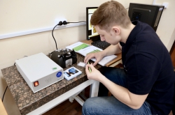
One way of detecting gases is altering the conductivity of the active layer adsorbing the gas molecules. The adsorbed molecules’ electric potential can influence the active layer charge carrier transport. It’s clear that in this case the thickness of the active layer should be brought to a minimum so that modifications in the electric potential of the surface would lead to a tangible change in the conductivity of the whole layer. That’s why gas sensors based on two-dimensional materials like graphene are highly sensitive to alien substances and thus can detect even the smallest traces of chemicals in the air. Aided by Professor Vladimir Pshenichnov and his second-year Faculty of Physics and Engineering assistant Tatiana Yurova, a group of summer camp participants were commissioned the task of designing such a gas sensor without the expensive high-tech equipment.

The student project team extracted the graphene by mechanical splitting using the sticky tape method pioneered by Nobel Prize laureates Andre Geim and Konstantin Novoselov. Students used the sticky tape to transfer several graphene layers to the template, but the trickiest part began when they had to measure the width of each piece of material to define what was graphene and what was graphite, as graphene is graphite’s atomic layer.
“This wasn’t simple as the students didn’t have the equipment that would allow them to discern between atomic and polyatomic layers. The team decided to circumvent this by using the light transmission intensity as an indication of a layer’s width. This meant that the kids had to teach themselves to estimate the number of layers with no special equipment apart from a simple optical microscope. This is a skill that only comes with experience. Then they had to affix the graphene surface with microcontacts so that recording devices could get the information of changes in graphene conductivity. It was difficult as the project team had to experiment with different methods and no one knew what would work. Many students got quite upset when things went wrong. Some stuck to one method and tried to improve it, others quickly switched to another. It was like real science,” said Vladimir Pshenichnov.
In their battle with graphene measurements the students explored numerous ways of depositing metal on phototemplate-based surfaces and sampled different techniques of creating sensor prototypes.
“There’s a fine line between the learning methods used at project-based bootcamps and academic competitions. While the latter predominantly focus on identifying promising students, the former aim at teaching them. There are no winners, everyone is involved in creating the final product. Some teams did it better, other teams did it worse, but all participants made significant personal progress. In other words, each student is talented, but in a different way, and it was the mentors’ task to understand this talent and help each person to develop it. That’s why all summer camp participant were winners, because they all managed to forge their own paths. Although all teams came up with a comprehensive nanotechnologies-based prototype, many students said that they would like to come to ITMO during their fall school break to perfect their projects,” observed Mikhail Mukhin, head of ITMO University’s Metamaterials Laboratory Nanocenter.

Summer camp participant Daria Kravtsunova said that her work on the project taught her to be independent and proactive when searching for problem solutions.
“We weren’t given a step-by-step plan of what to do, we had to make it ourselves. So we spent the first few days brainstorming ideas and developing our project agenda. We ended up doing everything on our own, from choosing the scientific methods to carrying out experiments and designing the prototype. For me this was the most important and valuable part of my summer camp experience. I did some micro and nanotechnologies project work last summer, but this time round I fully understood that there was much more to it than I’d ever expected. What’s more, I realized that there are so many unexplored scientific areas where I can make my contribution. In the words of Richard Feynman, there’s plenty of room at the bottom. I believe that advancing this line of scientific research can truly revolutionize our everyday lives. I’m fascinated by nanotechnologies and that’s why I intend to work in this field going forward,” shared Daria.
Another participant Ekaterina Smirnova adds that the project gave her the opportunity of trying her hand at the cutting-edge research equipment.
“We did a great deal of scientific work, but we were also taught to operate in laboratories, effectively delegate research tasks, interact within the team, and present our project in an appealing and accessible way. We live in an era of nanotechnologies, which open a whole new world of opportunities. In the future I’d like to continue researching nanotechnologies in ITMO University,” said Ekaterina.