Photovoltaics has become a relevant research field that all advanced countries are interested in. Where physics, photochemistry and electrical chemistry overlap, it researches the processes of electric currents' emergence in different materials under the effect of light. Presently, photovoltaics allows scientists from all over the world to discover new possibilities of using solar energy, most of which have to do with using thin-film systems.
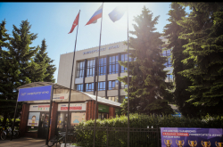
ITMO's new Organic Electronics and Photovoltaics Laboratory is not a classical laboratory like those they usually have at different universities. First of all, it is the result of collaboration of different industrial companies and ITMO University; also, other Russian universities contributed to its development. The laboratory's main goal is to conduct R&D in the field of organic electronics and photovoltaic materials and devices. Highly competent specialists took part in designing the laboratory - for instance, Dmitry Parashuk from Moscow State University, who came to the project about a year ago and now provides for the laboratory's science and technology maintenance.

"This is the first project in the field of photovoltaics and organic electronics that is being conducted in collaboration with industrial companies. What’s more, it has to do with not just any kind of photovoltaics, but thin-film photovoltaics in particular, which will then be used in such promising fields of technology as organic electronics and embedded photovoltaics. This is a new research field, which is why it is so important for ITMO to take part in working on such projects - the university has never done that before," says Viktoria Zheltova, director of ITMO's Engineering Center.
In general, the Laboratory focuses on the following fields: chemistry of liquids, coating and characterization. The laboratory is equipped with devices for spectroscopic measurements, as well as several MBRAUN workstations with vacuum cameras.

The new laboratory is also an example of an effective use of the university's resources. In the beginning of the year, the space now occupied by the laboratory was an old gym. In just four months, the organizers turned it into a multi-functional scientific environment.
"The main idea is that students and researchers who work here would have access to a full production cycle - from raw materials to the end product. Thus, the students will learn all of its stages. As of now, there are few organic electronics laboratories in Russia capable of this - the laboratory at Moscow State University, and the ones in Skoltech and Chernogolovka. There is something similar in Novosibirsk as well, yet that one does not feature a full production cycle. So, the major photovoltaic laboratories are concentrated around the capital. The new laboratory will be the first in St. Petersburg, though, naturally, there are already scientists who focus on organic electronics here. The field is really promising, as the application range is very wide: organic electronics devices, sensors and biosensors, devices for detecting X-radiation, fingerprint scanners and many more," explains Dmitriy Parashuk.

According to the laboratory's founders, the facility will focus on developing materials and concepts of devices. For electronics, that would be various displays and sensors, for photovoltaics, that would be flexible solar cell modules that can be applied on different surfaces.
"As we see it, the most rapidly developing field of photovoltaics application is everything that has to do with Energy independent electric vehicles. Some of those work on solar cells that are attached to the vehicles' surface. Another promising field is Energy harvesting. It has to do with using photovoltaics for charging mobile devices, sensors, everything that has to do with the Internet of Things and the like. We are also interested in Building-integrated photovoltaics, as well," comments Viktoria Zheltova.

At the ICOE-2017 conference in the beginning of June where the laboratory was first presented, Boris Galkin, Head of Russia's TEN FLECS Center for Organic Electronics, made a report on bridging the gap between R&D projects and mass production in the field of thin-film electronics prototyping and low-batch production.
"We believe that the laboratory at ITMO University is the first good example of a research facility that does not work on theoretical issues only, i.e. research for the sake of research, something we can't say we support and aspire to work with. We prefer working with those who can solve industry tasks and convert research into something that can be applied, i.e. conduct R&D that will be of interest to the industry. As we now launch contact manufacturing projects, it is most important to have an opportunity to test different new technologies, processes and materials on a laboratory level before introducing them into production," shared Boris Galkin.


